Test Point Altium Schematic
Test point altium symbol schematic create footprint designer testing created updated november april 2. schematic capture in altium designer Altium attached
How to Create a PCB Schematic | Altium Designer
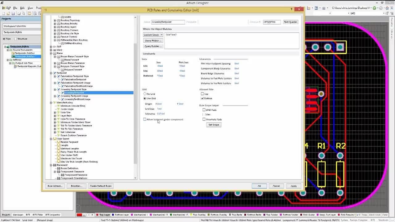
Altium designer pcb use test points point usages setting Altium pcb designer: test point manager design rules Altium designer testpoint pcb test points use menu setting styles
Altium test point designer
Altium pcb designer: test point manager design rulesAltium simulation circuits same better different project pass way simulated configuration various analysis filter made after high How to use pcb testpointsAltium schematic designer capture.
How to create a test point schematic symbol and footprint in altiumAltium scope Altium netsAltium pcb designer test points use thru manually testpoint setting hole.
How to use pcb testpoints
Altium pcb designer test use menu rules point pointsAltium designer in a minute: how to find all schematic nets How to use pcb testpointsAdding test-points.
How to use pcb testpointsFootprint test point altium schematic symbol create designer assign Altium designer schematicAltium designer tips #2: how to use test point manager.

How to create a pcb schematic
How to create a test point schematic symbol and footprint in altium .
.


How to Use PCB Testpoints | Altium Designer

How to Create a Test Point Schematic Symbol and Footprint in Altium

How to Use PCB Testpoints | Altium Designer

How to Create a PCB Schematic | Altium Designer

Altium - Simulation of different circuits in the same project. What's
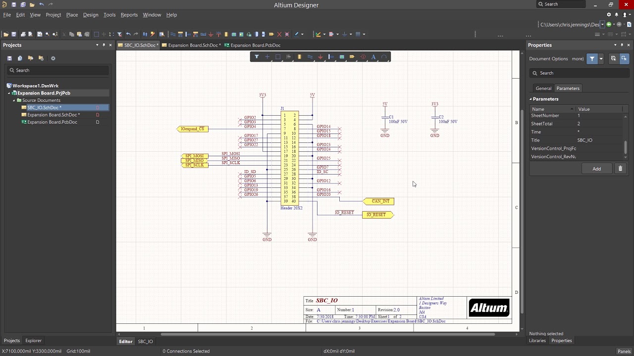
2. Schematic Capture in Altium Designer - YouTube

Altium Designer Tips #2: How to use Test Point Manager - YouTube

How to Use PCB Testpoints | Altium Designer

Altium PCB Designer: Test Point Manager Design Rules