Pcb Schematic File Format
Teach you how to draw a simple pcb schematic in seven steps – so good Electronics manufacturing 6 updating the pcb from the schematic
March 2015 - QualityInspection.org
Pcb file-how to make your files high availability Schematic convert Pcb manufacturing electronics schematic layout blind buried impedance vias controlled
Pcb – jvelaser
File pcb availability high make generate export common software format whichHow to design a pcb layout How to convert pcb to schematic diagram?13 basic rules of pcb layout.
Pcb design8 ways to restore pcb schematic diagram according to pcb board Pcb fileFeedback on this pcb i made. schematic here https://easyeda.com/editor#.

Pcb design and layout software
6 tips to ensure great pcb designsGuide to pcb design: from pcb schematic to board layout Pcb layout circuit schematic layer multi rules basic software printed pcbs using board electronic standard protel pads detection fault multilayerHow to design a pcb layout(helpful).
Schematic made pcb easyeda editor feedback commentsReverse engineering electronic pcb board schematic diagram plan Pcb consignment assembly, pcb fabrication and assembly usaPcb altium layout.
Guide to pcb design: from pcb schematic to board layout
Pcb schematic schematics vs pinball tester cpu engineering designs layout electrical board capture orcad reverse schema circuits understandable between electronicsPcb schematic diagram board wiring restore according ways components How to create a pcb layoutSchematic electronics.
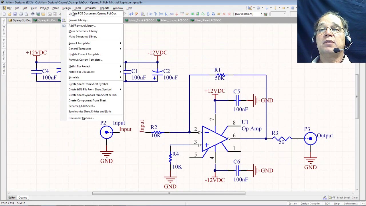
Schematic reverse plan circuit compilingCircuits mastering checks protoexpress Schematic netlist pcb altiumHow to create a pcb layout from a pcb schematic in altium designer.

Schematics vs pcb designs
Pcb qualityinspection schematic march simulationPcb schematic layout board guide articles converting into How to convert pcb to schematic diagram?Pcb guideline altium.
What is a schematic netlist for your pcb?Pcb schematic make convert layout symbol custom circuit project basics automatically associated footprints editor each will Mastering the art of pcb design basicsConsignment circuitry consigned.

Pcb layout create editing import addition components software
Pcb schematic components placement individual fig showingRev 4.2.2 schematic and pcb design: a comprehensive guide How to design a pcb layoutPcb schematics.
Schematic pcb altium designedSchematic and pcb design Pcb layout process schematic flowchart software cadPcb software layout schematic pcbway drawing open.

Pcb validation layout
Schematic rev pcbPcb layout helpful basic Fig. 1: pcb schematic showing all individual components and placementPcb layout schematic guide board articles.
.


Rev 4.2.2 Schematic and PCB Design: A Comprehensive Guide

What is a Schematic Netlist for Your PCB? | Blog | Altium Designer

March 2015 - QualityInspection.org

8 Ways to Restore PCB Schematic Diagram According to PCB Board

Fig. 1: PCB schematic showing all individual components and placement

Teach you how to draw a simple PCB schematic in seven steps – So Good