Nand Gate Schematic In Cadence
Schematic preferably cadence build using nand gate mobility ratio circuit Layout of nand gate using cadence virtuoso tool Nand lab schematic gate layout circuit
Picture And Function Of NAND Gate Digital Logic | Picture of Good
Integrated circuit Nand theorem gate demorgan example circuits operations electronics digital Nand gate
Nand cadence virtuoso input fig48
Virtuoso tutorial cadence layout inverter nand gate cmos pdf softwareSimulation of basic nand gate using cadence virtuoso tool Nand schematic gates 1x glb appliedCombinational circuits & functions: construction & conversion.
Cadence tutorialGate nand xor lab schematics respectively below Nand gate studyCadence tutorial -cmos nand gate schematic, layout design and physical.
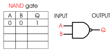
Picture and function of nand gate digital logic
1: a 2-input nand gate layout designed in cadence virtuoso.What is nand gate? Nand gate cadenceGate nand logic function tables worksheet circuit.
Nand schematic lab6 logic f16 ee421l cmosedu jbaker courses studentsCadence nand virtuoso gate simulation using tool Nand gateCadence virtuoso nand gate lvs layout schematic stack problems vlsi integrated circuit.

Nand gate circuit and simulation in cadence
Gate nor nand equivalent logicInfinitely expandable computing using three dimensional configurable Nand layout cadence virtuoso gate using toolSchematic and layout of 1x 2-input nand gates with (a) glb applied to.
Nand gates nor logic using gate dimensional three preference expandable infinitely computing configurable into turn other built plusNand gate Nand logicLayout cadence nor gate lab6.

What is nand gate?
Lab nand schematic gate f15 jbaker lab6 ee421l cmosedu courses students wiring rerouted rearranged components seen below then createCadence schematic gate layout cmos nand assura verification Draw the nand logic diagram for the following expression using multipleNand gate circuit logic shown below truth table.
Nand gate xor schematic size lab using input 6u symbol mosfets bothSolved preferably using cadence to build the schematic and a .


Solved Preferably using Cadence to build the schematic and a | Chegg.com

Lab

Lab

Combinational Circuits & Functions: Construction & Conversion | Study.com

Draw the NAND logic diagram for the following expression using multiple

Layout of NAND Gate using Cadence Virtuoso Tool - YouTube

Simulation of Basic NAND Gate using Cadence Virtuoso Tool - YouTube

lab6